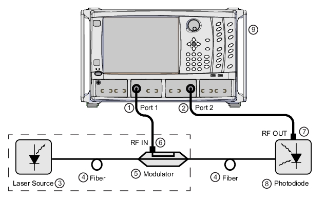
Conceptually, the job of the optical modulator is to place a microwave signal as modulation onto an optical carrier. Similarly, the job of the photodetector or receiver is to recover that modulation and regenerate the microwave signal. For a VNA-based measurement, both directions of conversion are required so that the processing can occur in the microwave or modulation signal domain. The result is a setup like that shown in Figure: General 2-Port E/O or O/E Measurement Setup (a MS464XX VNA is shown in the image, but a broadband system ME7838XX can be used as well). The optical carrier is generated (usually) by a coherent laser source (which may be integrated with the modulator), modulation is applied, and then the modulation is recovered. Optical fiber is shown as the media in Figure: General 2-Port E/O or O/E Measurement Setup but it could be some other optical guiding medium or free-space in some cases. The VNA acts as a microwave stimulus (Port 1 in the figure) and receiver (Port 2 in the figure). 3- and 4-port cases are also possible, involving multiple converters or differential ones, which will be discussed later in this chapter. Although a fiber is shown as the only element between the detector and modulator in Figure: General 2-Port E/O or O/E Measurement Setup, some optical DUT may be there for O/O measurements.
General 2-Port E/O or O/E Measurement Setup
Index
Description
Index
Description
1
VNA Port 1
6
Modulator RF IN
2
VNA Port 2
7
Photodiode RF OUT
3
Laser Source
8
Photodiode
4
Fiber
9
MS464xB VNA
5
Modulator
In some cases, the laser and modulator may be one assembly (as is the case in the MN4775X converter). The photodiode may be integrated with amplifiers or other components into a photoreceiver.
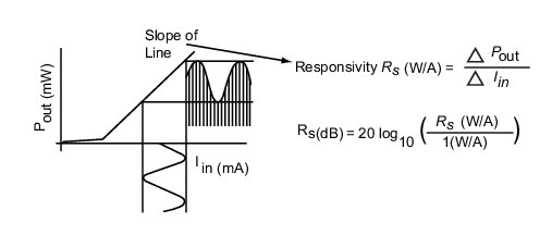
Since the measurements results will be classed as normal S-parameters, one may wonder how these relate to the actual optical behaviors of the components. In some sense, they all become relative because the conversion between domains introduces dependencies on optical laser power, optical path losses (usually small) and other absolute shifts. Thus the real measure of conversion is essentially a responsivity slope between the optical and electrical domains as illustrated in Figure: Responsivity Concept. The S-parameters that appear on the instrument display for an O/E or an E/O component then represent a relative responsivity measure (in both magnitude and phase). Often, the frequency response of this quantity is of interest as that determines bandwidth and magnitude vs. frequency plot gives this information. The phase linearity and group delay are both ways of looking at the deviation from a purely linear phase function that can be an important assessment of potential phase-related modulation distortion. Return loss of the component may also be of interest but that is a purely microwave measurement.
Responsivity Concept
The conversion parameters of the O/E and E/O devices measured with the VNA are essentially measures of responsivity.
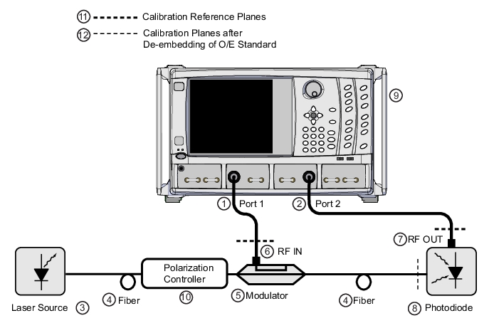
A next question may be how the measurements are conducted. The starting point is a 2-port VNA calibration as has been discussed in earlier chapters of this measurement guide. This calibration establishes reference planes at the microwave ports of the optical devices as shown in Figure: Reference Plane Placement (often coaxial ports but could be waveguide, in a fixture, etc.). The next step is the use of an O/E calibration device such as the MN4765X. That particular model is a wide bandwidth photodetector housed in a thermally controlled module with carefully designed bias circuitry. This module is characterized at a traceable facility using electro-optic sampling techniques (or references derived from that) so its frequency response (in magnitude and phase) is well-known with established uncertainties (e.g., [1] -[2]). If such a calibration device is the detector in Figure: General 2-Port E/O or O/E Measurement Setup, then its effects can be de-embedded (see the embedding/de-embedding sections of Calibration and Measurement Enhancements in this guide for more general information) since those behaviors are known. This then moves the reference plane to the optical side of the photodiode/calibration detector as shown in Figure: Reference Plane Placement. Now a measurement of S21 will describe the loss and phase of the modulator alone (plus some effect of the fiber which will be discussed). This frequency response (magnitude and phase) gives the required performance information discussed earlier when combined with the microwave reflection measurement (S11 in the diagram) of the modulator RF port that comes for ‘free’ with the calibrated VNA measurement.
A polarization controller is shown in Figure: Reference Plane Placement but, technically, this is optional. Many modulator structures (including Mach-Zehnder modulators such as those used in the MN4775X converter), are polarization sensitive so at least a polarization-maintaining fiber is recommended on the modulator input.
Reference Plane Placement
Index
Description
Index
Description
1
VNA Port 1
7
Photodiode RF OUT
2
VNA Port 2
8
Photodiode
3
Laser Source
9
MS464xB VNA
4
Fiber
10
Polarization Controller
5
Modulator
11
Calibration Reference Planes
6
Modulator RF IN
12
Calibration Planes after de-embedding of O/E Standard
A calibration is done in coax, waveguide, or some other electrical media and the de-embedding function, via the O/E-E/O measurement utility, of the VNA are used together with optical data to move a reference plane into the optical domain.
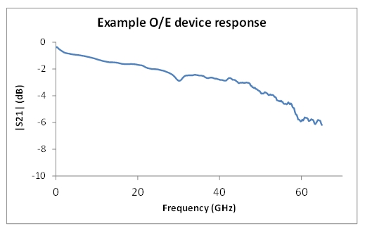
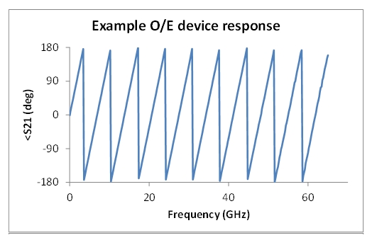
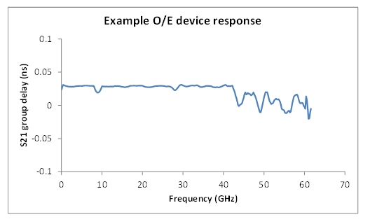
An example plot of the conversion response of a 50 GHz photodetector is shown in Figure: Characteristics of Example O/E Device. From the magnitude response, the 3-dB bandwidth is indeed around 50 GHz but the roll-off is sufficiently slow that this device is commonly used beyond 65 GHz. The phase response is also shown in the figure but the linear portion has not been removed. The group delay plot (derivative of phase with respect to frequency) is often a more convenient way of looking at the phase behavior. Towards 50 GHz, there are some deviations from flat group delay (equivalent to deviations from linear phase) that are not surprising in view of the device’s bandwidth. If being used as a characterization device, these deviations are not important since they can be well-characterized (to beyond 65 GHz in this case).
Characteristics of Example O/E Device
If one now wanted to measure a different O/E device (not a calibration module), one could then insert that detector into the setup of Figure: Reference Plane Placement and instead now de-embed the modulator response that was just found. In this case, because it is a second level de-embed, there may be some elevation of uncertainties that will be discussed. One could also obtain an E/O calibration device and use that instead in a one-step process.
The de-embedding (or sequential de-embedding) steps form the basis of this O/E-E/O measurement utility. The key points are controlling traceability and uncertainties throughout the process when multiple devices are being used, to control match so minimal additional artifacts are introduced, and to not try to de-embed what cannot be de-embedded. This last point is important in that inner-plane (optical) match is not known and the transmission path is unilateral anyway, so there are no multiple reflections within the DUT assembly to remove.
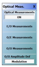
Optical Measurements Menu
All of these measurement aids are available under the Perform Optical Measurements button located on the MEASUREMENTS menu (Navigation: MAIN | Measurement | MEASUREMENT | Optical Measurements | OPTICAL MEAS. menu). As might have been guessed from the previous discussion, these approaches naturally separate based on whether the target is an O/E device (e.g., detector or receiver), an E/O device (e.g, modulator), or an O/O device (e.g, coupler, amplifier, or filter, etc). The menu selections, as shown in Figure: OPTICAL MEASUREMENTS Menu delineate that choice.
OPTICAL MEASUREMENTS Menu
On the Optical Measurements menu are the three selections based on which type of device is to be solved for.
A certain class of purely optical (O/O) measurements can also be made where both the detector and the modulator have been de-embedded. One essentially performs the steps for both the E/O and O/E measurements in series to place the reference planes in the optical domain. This is still a microwave/millimeter wave frequency response measurement, so the O/O measurement is really a measure of the response to changing modulation bandwidths and, as such, is most suited to relatively narrowband optical devices such as amplifiers, filters, couplers, resonators, etc. For example, it would be unusual for a patch cord to show variation over a millimeter wave modulation bandwidth (unless it had some particularly unusual distortion properties). Also, mismatch in the optical domain is not correctable with this technique and, if the fiber runs are long, it is possible that ripple will occur on the scale of millimeter wave frequencies. An additional complication with the O/O measurements is the difference between modulation domain power detected by the VNA receivers and optical power. The issue comes about because the O/E detector or calibration module is essentially a square-law device taking optical power changes to root-power (or normalized voltage). The default O/O readings will be in the modulation domain, which may represent double the loss (in dB terms) from what would be seen with an optical power meter. Thus an optical power choice is available for O/O measurements that will scale the results appropriately when thinking in terms of optical carrier power. Note that this correction happens after all calibrations have been applied, but before post-processing. So if one is using trace math normalization to help evaluate, for example, optical device loss, the normalization should be done in the same state (modulation domain or optical power) as the measurement.
All of the measurements (up to this point) in this chapter work by using information about optical converters to modify an RF calibration coefficient set on the VectorStar VNA. This is exactly how conventional de-embedding works but the optical variants of this process take additional steps to handle the unilateral nature of the optical system (one cannot apply RF to the detector and usually expect RF to be produced by the modulator) and some differences in match terms. As with regular de-embedding, the optical modification to the calibration coefficients can be turned on and off. Turning the Optical Measurements to OFF will cause the original RF calibrations coefficients to be loaded. Returning Optical Measurements to ON will reload the modified coefficients. Both sets of coefficients are stored as part of the setup file.
While the bulk of the optoelectronic functionality is intended to measure the RF (modulated) response in converting devices and optical systems, it is also possible to measure effects on average optical power (the 'carrier' in this measurement class). This can be useful to get a quick estimate of laser or OE/EO behavior, optical path losses, or interconnect issues. The simplest method using the VNA is to plot average optical power directly. While akin to what an optical power meter can do, this measurement is based on OE module DC output. The accuracy will not be as high as for a dedicated optical power meter but it does have the ability to reveal effects from the RF system as well be discussed.
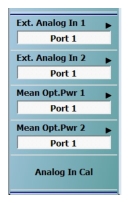
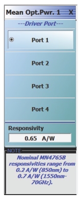
The lower part of the RESPONSE menu when in an optoelectronic mode is shown here. Mean optical power can be selected as a response variable (two inputs are available). The RF driving port must be selected and the detector responsivity entered.
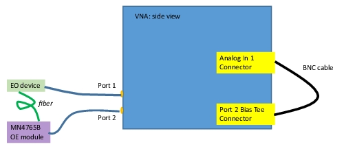
Note that are two Mean Optical Power selections available since there are two Analog In ports on the VNA. Thus, the optical power from two different points in a setup, assuming detectors are available, can be measured simultaneously along with the S-parameters. External Analog In response parameters can still be selected and these will plot raw voltages at the analog in ports.
One connection arrangement for optical power measurements is shown here. The DC detector output must get to one of the Analog In rear panel connectors and using the internal bias tee and a BNC cable is one approach.
• The responsivity of the detector must be known (in A/W). Typical values for the Anritsu MN4765B are shown below but this can also be computed by using the straight analog in measurement (not the optical power response selection) and a measurement with an optical power meter if greater accuracy is desired. See Figure: MEAN OPT. PWR. submenu where responsivity can be entered. for the sub-menu where responsivity is entered.
OE module
Typical responsivity (A/W)
Comments
MN4765B-004x
0.2 (at 850 nm)
0.6 @ 1060 nm, 0.7 @ 1310 nm, 0.8 @ 1550 nm
MN4765B-0070
0.7
MN4765B-0071
0.45
MN4765B-0072
0.65 (at 1550 nm)
0.45 @ 1310 nm
MN4765B-011x
0.55 (at 1550 nm)
0.25 @ 1310 nm
MEAN OPT. PWR. submenu where responsivity can be entered.
• Other OE devices can act as the power detection conduit, but the responsivity must also be known, the output DC levels must be in the range of the Analog In port (-5 V to +5 V), and a 50 ohm terminating resistor in the OE device is assumed (since only voltages are measured by the analog in port). Accuracy of the DC measurement is on the order of 0.5 mV (additive) so very low responsivity detectors will produce mean optical power measurements with higher uncertainties.
• As suggested by Figure: MEAN OPT. PWR. submenu where responsivity can be entered., the driver port must be selected. This is the RF driving port that will be associated with the DC measurement and will almost always be the port to which the EO device is connected.
• The signal levels measured are typically in the mV range for common optical power levels so the calibration of the Analog In port can be relevant. While this calibration happens automatically at application launch, the values can drift somewhat over time if the instrument is left running for extended periods. A calibration button is available on the response menu to refresh this state. This calibration re-zeros and recomputes the gain corrections of the low frequency analog in paths.
• In some extended-length setups, ground voltage imbalances can occur which complicate the mV scale measurements at low optical power. Additional grounding paths (e.g., ground straps or cables) may be needed from the detector plane to the VNA to get accurate low optical power readings.
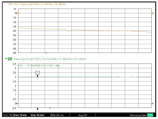
An example optical power measurement (trace 2) is shown here as part of an EO measurement setup. The Power Out graph type is particularly convenient.
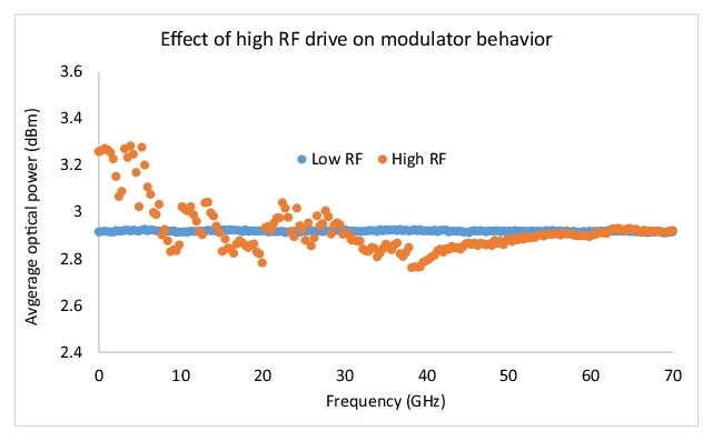
If some part of the item being measured is interacting nonlinearly with the RF signal, variation over the sweep may be observed. One example is with a Mach-Zehnder EO device where the RF amplitude is on the same order as the Vπ, or modulation swing range, of that modulator. In this case, the RF can alter the bias state of the device and the mean optical power getting to the detector can vary widely. An example of such a situation is shown in Figure: An example where the swept nature of the optical power measurement can be useful: observing RF-related nonlinear effects of the DUT structure. where the RF was applied through an amplifier that had more gain at lower frequencies and, for the high drive example, was able to compromise the bias state of the modulator at those frequencies. The net optical power deviation was not large in this example, but multi-dB swings are possible for some configurations.
An example where the swept nature of the optical power measurement can be useful: observing RF-related nonlinear effects of the DUT structure.
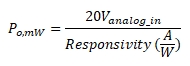
The optical power uncertainty from this measurement is limited by the accuracy in the knowledge of the responsivity and the accuracy of the DC voltage measurement. For an Analog In port with a current calibration, the latter uncertainty is typically 0.5 mV assuming no ground distortions are present. The optical power in mW is computed as
So, if the responsivity is very low, the Analog In voltages will be lower (for a given optical power) and the DC measurement accuracy will have more of an effect on the computed optical power.